Scientists of South Ural State University created the newest program for optimization of photonic crystals’ structure. The program allows for solving the problem on optimal atom arrangement and accelerating the process of creation of a ‘perfect’ photonic crystal.
Research group headed by Professor of the Department of Optoinformatics of the SUSU Institute of Natural Sciences and Mathematics’ Faculty of Physics, Yuriy Miklyaev, has been studying photonic crystals for many years. Photonic crystals are not just able to replace traditional elements of optical systems and expensive rare earth metals, but to become the basis for photonic integrated circuits – elements of a supercomputer of the future, and thus become a breakthrough in the 4th scientific and technological revolution. In co-authorship with Denis Pikhulya he wrote the program on “Optimization of photonic crystals’ structure by the method of mode confinement in the corresponding medium”.
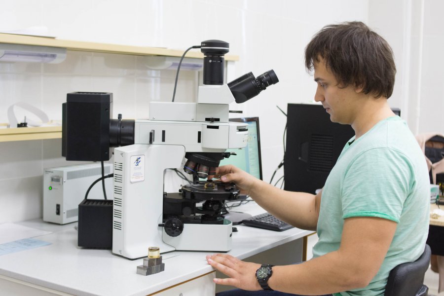
“Creation of three-dimensional photonic crystals can be conventionally divided into several stages,” says Yuriy Miklyaev. “During the first stage work physicists-theorists and programmers. Their goal is to elaborate a structure that will most efficiently perform the function of a photonic crystal, i.e. permit or not permit light through in a certain direction. A computer program that calculates millions of variants gets created. Here at SUSU we use the power of supercomputer to solve such complicated problems, which allows achieving significant results. The result of this meticulous work was creation of a new program for solving the problem on optimal atom arrangement in a photonic crystal.”
.jpg)
At the moment, properties of photonic crystals are being actively studied at South Ural State University; theoretical methods of their research are being developed; various devices containing photonic crystals are being developed and researched; and the effects theoretically predicted in them are being implemented in practice.
“Photonic crystals are a term that appeared in science more than 40 years ago,” explains the SUSU scientist. “Theoretically, it has been proved that by controlling the structure of various materials and shaping it in a certain way it is possible to obtain a unique control over the electromagnet wave that is distributing in this medium. In other words, photonic crystal is a material which can control electromagnet waves and lead to formation of some kind of a filter – the photonic band gap.”
Due to their amazing properties, photonic crystals provide principally new possibilities for controlling light fluxes. There are optical filters, waveguides (particularly in fiber-optic communication lines) and devices allowing to control thermal radiation, which are created and developed on the basis of photonic crystals.
The future of modern electronics is connected with photonic crystals. Ideology of photonic structures lies in the basis of creation of nonthreshold semiconductor lasers, the lasers on the basis of rare earth ions. Materials of the new generation will allow for creating optical microcircuits based on the sort of elements of semi-conductor electronics; and principally new methods of transmission, storage and processing of information, which are nowadays get tested with the use of photonic crystals will become applicable in semiconductor electronics of the future.
The program of “Optimization of photonic crystals’ structure by the method of mode confinement in the corresponding medium” has already received certificate of registration, but the scientists are still to solve a lot of complex problems. In order to develop photonic crystals of high quality, a material with a certain refraction index is required, including diamond and titanium dioxide. It is very hard and sometimes impossible to produce free structures out of them, especially three-dimensional structures. Nevertheless, the SUSU scientists keep searching for ways to overcome the obstacles made by the nature.